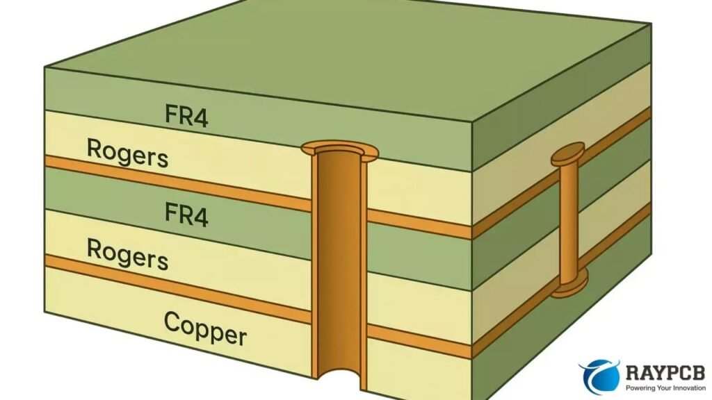
Very few products need high-frequency laminate on every layer. A typical RF board has an antenna or front end that genuinely requires controlled dielectric performance, sitting above a digital section, a power distribution network and a handful of ground planes that would be perfectly happy on FR-4. Hybrid construction exploits that, placing expensive material only where it earns its cost. Done well it delivers most of the electrical benefit at a fraction of the price. Done carelessly it produces warped boards, cracked vias and impedance that will not repeat.
Why hybrids are worth the trouble
The cost argument is the obvious one. High-frequency laminate can run several times the price of FR-4 per unit area, so restricting it to two layers out of eight removes most of the material premium. But cost is not the only reason.
Mechanical rigidity matters too. PTFE-based laminates are soft, and a board built entirely from them flexes in ways that complicate assembly and connector retention. FR-4 cores in the middle of the stack provide structure that pure PTFE constructions lack. There is also a thermal argument: FR-4 layers give the fabricator familiar material to work with in the bulk of the stack, which usually improves registration and yield relative to an all-PTFE build of the same layer count.
The bonding problem
The central technical question in any hybrid is what holds the dissimilar materials together. Standard FR-4 prepreg does not bond reliably to fluoropolymer surfaces, and the lamination temperature and pressure profiles for the two material families are different enough that a single press cycle cannot be optimal for both.
For RO4000-series hybrids, RO4450F bonding prepreg is the material designed for exactly this job. Its significant advantage is that it laminates at temperatures close to standard FR-4 processing, which means the whole stack can go through one press cycle without subjecting the epoxy layers to conditions they were not designed for. Its dielectric properties also sit close enough to the RO4000 cores that the bonded composite behaves predictably in a field solver.
For PTFE-based hybrids involving RT/duroid or RO3003, the problem is harder. Those materials need surface activation before anything will bond to them, and their lamination requirements diverge further from epoxy. Constructions in this family often require sequential lamination — building the PTFE section first, then bonding it to the FR-4 section in a second cycle — which adds cost and lead time but avoids forcing a compromise press profile on both halves.
Coefficient of thermal expansion mismatch
This is where hybrid constructions fail, and it is the issue least often discussed at design review.
The z-axis thermal expansion of PTFE-based laminate can approach 237 ppm/°C. FR-4 sits nearer 50 to 70. Bond those together and every thermal excursion — lamination, reflow, rework, field temperature cycling — puts the interface under shear stress, because one side wants to grow several times more than the other.
Two consequences follow. First, any plated via crossing the boundary experiences barrel strain concentrated at the interface, which is where barrel cracks initiate. Second, if the stack is not symmetrical about its centre, the differential expansion bows the board. A hybrid that looks elegant on a stackup drawing and ignores symmetry will come back from lamination with a warp that no amount of baking removes.
Design rules that prevent the common failures
- Keep the stackup symmetrical about the centreline in both material distribution and copper weight. Asymmetry and CTE mismatch together guarantee warpage.
- Minimise the number of plated vias crossing a material boundary. Where a transition is unavoidable, consider whether the signal can change layers within one material section instead.
- Specify plating thickness on the higher end of the acceptable range for vias crossing the interface, since barrel strength is what resists the differential expansion.
- Place the high-frequency material on outer layers where practical. This simplifies bonding, keeps antenna structures accessible, and avoids burying the difficult material in the middle of the stack.
- Confirm whether the construction needs sequential lamination before quoting, because it materially changes both cost and lead time.
- Ask for pressed thicknesses rather than nominal ones. Different materials compress differently, and the difference is where impedance error lives.
Via structures across material boundaries
Signal transitions in a hybrid deserve more thought than in a homogeneous board, because a via that crosses from one material into another crosses a discontinuity in both dielectric constant and mechanical behaviour.
Electrically, the dielectric constant seen by the via changes partway down its length, which produces a small impedance step. At low frequency this is invisible. Above roughly 10 GHz it becomes part of the loss and return-loss budget, and it is one reason designers prefer to keep high-frequency signals within a single material section and route only lower-frequency signals through the boundary.
Mechanically, the same via sits at the point of maximum shear during thermal cycling. Back-drilling stubs, which is standard practice on high-speed digital designs, needs particular care here: the drill depth tolerance interacts with the differing thickness behaviour of the two materials, and an aggressive back-drill specification that is routine on FR-4 can become a yield problem on a hybrid.
A representative construction
| Layer | Material | Function | Note |
| L1 | RO4350B | RF traces, antenna | Controlled impedance |
| L2 | RO4350B (same core) | RF reference ground | Solid plane, no splits |
| — | RO4450F bondply | Bonding layer | FR-4-compatible cycle |
| L3–L6 | FR-4 cores | Digital, power, ground | Bulk of the stack |
| — | RO4450F bondply | Bonding layer | Maintains symmetry |
| L7–L8 | RO4350B | Second RF section | Mirrors L1–L2 |
The structure above illustrates the principle rather than prescribing a specific design: high-frequency material on both outer sections, FR-4 through the middle, identical bonding layers at symmetric positions. If your design needs RF on only one face, the usual approach is to balance the stack with a dummy layer of the same material rather than accepting an asymmetric build.
Warpage and how it shows up
Warpage from a hybrid construction rarely announces itself at the fabricator. Boards leave inspection flat enough to pass, then bow during reflow when the differential expansion is driven hardest. The symptom appears at assembly as inconsistent paste deposition or open joints under larger packages, and it gets attributed to the assembly process rather than the stackup.
If a hybrid design is showing assembly yield problems that nobody can pin down, measure board flatness before and after a thermal cycle rather than only on incoming inspection. A construction that is flat cold and bowed hot is telling you its stackup is not balanced.
Reference plane discipline
One rule survives from conventional design and matters more here: the reference plane directly beneath a high-frequency trace must be solid and unbroken. A split, a routing channel or an antipad cluster under an RF line forces return current to detour, which raises impedance discontinuity and radiates.
In hybrid stacks this becomes easier to get wrong, because the tempting place to route dense digital signals is exactly the FR-4 layer sitting under the RF section. Assign that layer as dedicated ground and route the digital signals deeper. Any experienced Rogers PCB fabricator will flag the problem during design-for-manufacture review, but it is far cheaper to catch during layout than after the first article arrives.
Lead time and cost expectations
Hybrids sit between pure FR-4 and pure high-frequency construction on both cost and schedule, but not always where intuition suggests. Where the whole stack can be laminated in a single cycle using an FR-4-compatible bonding prepreg, the cost premium over a conventional board is largely the material itself. Where sequential lamination is required, the board goes through the press twice, which adds a meaningful increment to both price and lead time.
This is worth establishing early, because it is often possible to restructure a stackup so that a single lamination cycle becomes viable. Moving the high-frequency section to the outer layers rather than burying it is the most common change, and it typically costs nothing in electrical performance while removing an entire process step.
What to send with the RFQ
Hybrid constructions are quoted badly when the fabricator has to guess. Include the intended material for every layer rather than only the high-frequency ones, the bonding material if you have a preference, the impedance targets with the reference layer identified for each, the copper weight per layer, and an explicit note about whether sequential lamination is acceptable to you.
Ask the supplier to return a proposed stackup with pressed thicknesses and their own impedance calculation before you commit. Where their numbers differ from yours, the discussion that follows almost always surfaces a design-Dk assumption or a pressed-thickness estimate that one side had wrong. Choosing a Rogers PCB manufacturer willing to have that conversation before tooling is worth more than a small difference in unit price.
Closing
Hybrid stackups are the default answer for most commercial RF products, not a compromise. The engineering that makes them work is unglamorous: symmetry, bonding material selection, via placement relative to material boundaries, and honest pressed-thickness data. Get those four right and the construction is routine. Ignore any one of them and the failure usually appears after assembly, when it is most expensive to fix. https://techinfobusiness.com/